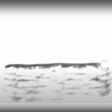
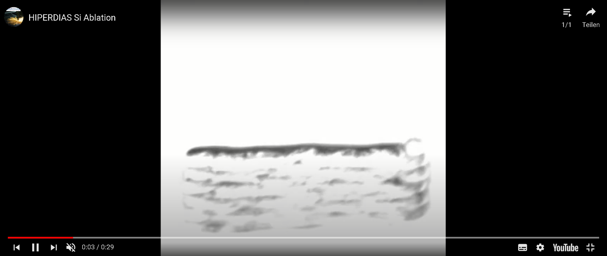
This video shows the surface of a polished silicon wafer is shown on which a rectangular structure with the footprint of 1x1 mm² is to be ablated with a USP laser. The ablation process can then be seen on a time scale in which the behaviour of the galvo scanner is easily comprehensible and shows a bidirectional scanning strategy. The step by step building up lines correspond to many single ablation events, which form the lines with a certain overlapping. The lines themselves are then arranged with an overlap so that they form full areas in one overscan. One overscan is completed in approximately 20 milliseconds, from overscan to overscan it becomes apparent that the depth of the structure increases. The process parameters applied result in a smooth surface without any deterioration, with an average laser power of about 50 W. Thanks to David Brinkmeier for recording this video as part of his Master’s thesis at BOSCH in Renningen, Germany.