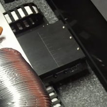
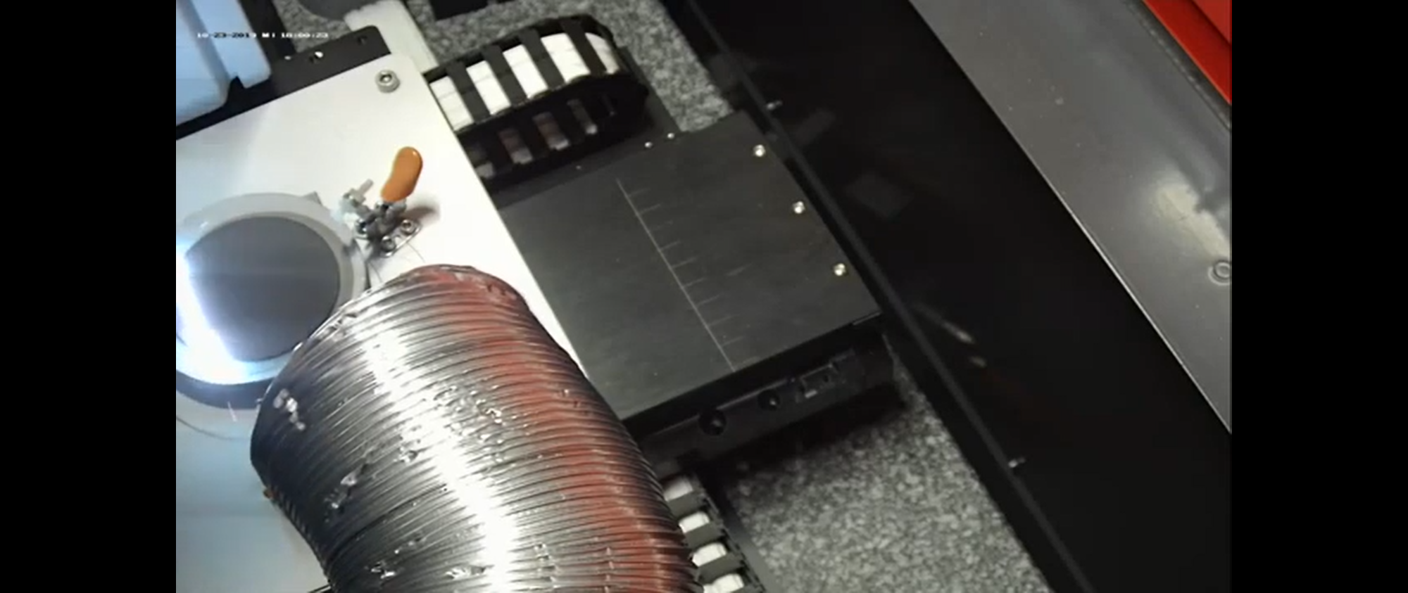
This video shows laser ablation trials carried out on PCD wafer with a high-power femtosecond laser system (990 W on the workpiece with a minimum pulse duration of 500 fs). The laser was developed by USTUTT, with these experiments taking place at USTUTT. The aim of these trials is to reduce the roughness of the top surface of the PCD wafers to the lowest possible, anticipating 5 time reduction in processing time compared to current methods.